Raising the Bar on Bias
Posted January 08, 2024 by Juergen Braun
The semiconductor industry thrives on challenge. It consistently achieves what was once considered impossible, overcoming obstacles previously seen as unassailable. The industry has proven time and time again that near-term limits can be overcome with technology advances. This has enabled continual chip size reduction while increasing density to deliver better efficiency and higher-speed devices.
In fact, relatively recent advances at micron, sub-micron and nanometer nodes will soon be surpassed as technology enters the Angstrom Era — with feature size dimensions measured in tenths of a nanometer (10-10 m). At the same time, designs are becoming more complex, leading to 3D and high-aspect-ratio structures with increasingly precise specifications.
Faster. Smaller. More Efficient.
How does the industry continually make these leaps?
It requires visionary process innovations supported by tightly controlled, customizable source and bias power delivery for plasma-based processes used to create today’s and tomorrow’s most advanced chips. Specifically, etch processes must produce pristine features with increasingly stringent characteristics.
A leap ahead in powered bias technology is key to accomplishing these imperatives for both critical etch and deposition processes.
Conventional RF Approach
The scaled, multi-frequency approach to bias is reaching limits in its effectiveness to specifically control critical wafer-level reactions. Because this method utilizes multiple interacting frequencies to influence specific ion energy distribution levels, its ability to independently control energy distribution mean and spread is limited.

Furthermore, conventional RF bias systems are becoming more complex. Process engineers require higher energy, voltages, and more frequencies to produce high-aspect-ratio and sub-nanometer dimensions. As this method scales up, this excessively increases:
• Costs
• Absolute power levels
• Requirements for synchronization of all power sources
Selection of Narrower Ion Energies
Considering the limitations of RF bias, what’s the next step in bias technology?
 eVoS™ ME
|
AE’s new eVoS™ Asymmetric Bias Waveform Generator directly controls wafer-bias voltage. Its tailored waveform produces narrow ion distribution, pinpoint energy precision and accuracy, and the ability to tailor ion energy selection/distribution. The resulting enhanced etch selectivity enables the most precise, customizable device feature formation.
.png "eVoS_FR_T-(1).png") eVoS™ LE
|
The eVoS system includes an agile high-voltage power supply combined with an innovative asymmetric waveform generating technology to establish and control wafer surface potential. Its asymmetric output eliminates the limitations and restrictions of wafer biasing inherent to sinusoidal RF bias generator and impedance matching installations. Fast digital metrology and novel control algorithms enable ion energy distributions that approach near mono-energetic levels.

AE’s eVoS technology also enables a more streamlined, controlled bias design compared to RF techniques.

Further, synchronization with the eVerest™ RF generator, used as source power, is built into eVoS by design. This ensures precise power delivery at the timing and at the levels required to effectively create the desired feature. During deposition, it also helps cover features uniformly.
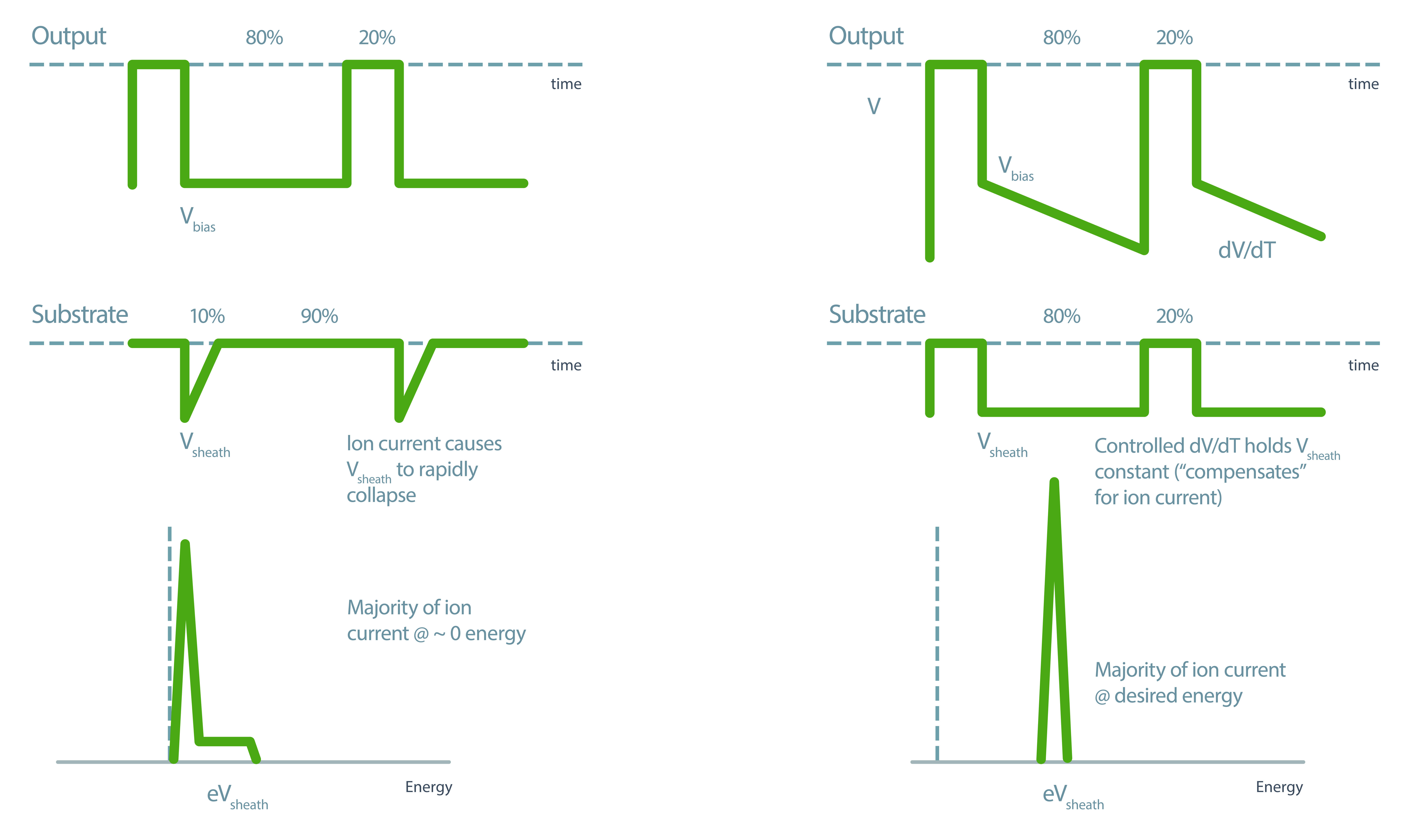
What about using a pulsed-DC power supply to control wafer-bias voltage? In addition to the eVoS platform’s advantages over RF approaches, its patented switch mode bias and control provides multiple benefits over a limited pulsed-DC bias approach by:
- Periodically resetting surface charge by positive voltage reversals
- Establishing user-defined bias voltage
- Holding substrate voltage constant (enabled by controlled dV/dT from the power supply) to achieve desired ion energy distribution
.jpg "scheme_Pulsed-DC-Waveform_eVoS-Waveform-copy-(1).jpg")
Bias Technology that Supports Extraordinary Ingenuity
History has proven that advances in chip technology require leaps forward in process and equipment design. AE’s eVoS Asymmetric Bias Waveform Generator, and the new eVerest RF Generator with the Navigator® II MLP Match, are leading examples of the innovation that has come to define the semiconductor industry.
Learn More About the eVoS Asymmetric Bias Waveform Generator.
Learn More About eVerest RF Generator.