Fine-Tuning for the Future: Enhancing Plasma Processes with Impedance Matching Networks
Posted December 14, 2023 by Niraja Bhalchandra
In the realm of semiconductor manufacturing, where precision and control are paramount, RF impedance matching networks play a critical role. These networks act as a bridge between the plasma source and the process chamber, optimizing power transfer and ensuring stable and efficient semiconductor processes.
This blog delves into the concept of impedance matching networks and explores their significance in semiconductor manufacturing. It demystifies the underlying principles, discusses key components and their limitations, and sheds light on how they contribute to maximizing the performance and reliability of semiconductor processes.
Impedance mismatch can lead to reflections, standing waves, and instabilities in the process. These can result in non-uniform plasma distribution, reduced process repeatability, and compromised device performance.
The impedance matching network acts as intermediary between the power source and the load in a semiconductor process.
Most power sources are designed to operate into a 50 Ω load, which is the industry standard for measuring and transferring high-frequency electrical power. The function of an impedance matching network, then, is to transform the resistive and capacitive characteristics of the plasma to 50 Ω, thus matching the output impedance of the power source and the input impedance of the load, typically a plasma chamber or a device under fabrication. Minimizing mismatch helps increase stability and consistency in semiconductor processes. The goal is to achieve efficient power transfer, which is crucial for achieving desired process outcomes.
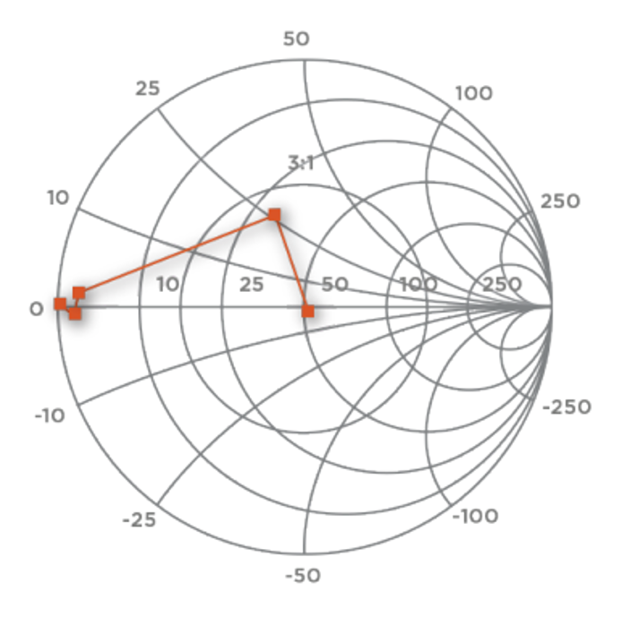.png "1-(1).png")
Figure 1. Smith® Chart showing matching network transforming plasma impedance characteristics to 50 Ω
Furthermore, fine-tuning the matching elements helps optimize plasma density, ensuring consistent etch rates, uniform film thickness, and improved process reproducibility.
The match also acts as a safeguard for the RF power supply. It prevents reflected power from reaching the power supply, minimizing voltage standing wave ratio (VSWR) alarms and potential damage to the RF components.

While a transformer is the simplest solution to match the impedance of the load and the power source, it is generally limited and only used in the simplest semiconductor manufacturing processes. On the other hand, impedance matching networks offer substantially greater capabilities and flexibility, and are most commonly used in plasma-based semiconductor manufacturing processes.
Within a conventional matching network, capacitor and inductor components are strategically selected and arranged to achieve the desired impedance transformation required to match the load impedance.
Designing an impedance matching network requires a deep understanding of the characteristics of the power source and load. Factors such as the operating frequency, power level, and desired bandwidth need to be considered. Additionally, the network should be designed to minimize losses and maintain stability under varying process conditions.
A well-designed impedance matching network facilitates scalability, allowing seamless integration into different equipment configurations and enhancing manufacturing flexibility.
Conventional networks are typically made of passive components — capacitors and inductors. These components ensure the network transforms the network impedance to match the load impedance. Conventional networks face certain limitations that hinder their performance and adaptability in future plasma processing technologies:
Frequency Limitations: Existing passive impedance matching networks are designed for specific frequencies, limiting their use to a narrow range of applications. As the semiconductor industry evolves, with new materials and processes emerging, the need for broader frequency ranges becomes crucial.
Complex and Dynamic Environments: Semiconductor plasma systems operate in dynamic environments with varying process conditions. Plasma impedance can quickly change due to factors such as temperature, pressure, and gas composition. Passive impedance matching networks struggle to adapt to these changes, leading to reduced efficiency and reliability.
Miniaturization and Integration: The continuous demand for smaller and more compact plasma processing equipment poses challenges for traditional impedance matching networks, which often require bulky and discrete components. Achieving miniaturization and integration is essential for next-generation plasma devices.

AE’s Navigator® II FCi
Navigator® II FCi is a standalone impedance matching network incorporating tuning elements adjusted by discrete solid-state switched capacitor arrays. It is driven by the need to achieve fast, accurate tuning across wider impedances. These matches have similar forms, footprints, and tuning ranges as their traditional counterparts, but offer tuning times in the millisecond range compared to the typical one-second range. This new high-speed matching technology is optimized and suited for critical power-sensitive, short-duration plasma process steps.
As the semiconductor industry continues to push the boundaries of miniaturization and performance, impedance matching networks will play a crucial role in ensuring optimal power delivery and uniformity in thin-film deposition processes. In the Angstrom Era, their significance in achieving superior process outcomes will only grow.

AE continues to advance adaptive matching techniques, wideband capabilities, integration with process control systems, and data insights to enable more precise, efficient, and controlled performance – helping enable visionary semiconductor processes.
This blog delves into the concept of impedance matching networks and explores their significance in semiconductor manufacturing. It demystifies the underlying principles, discusses key components and their limitations, and sheds light on how they contribute to maximizing the performance and reliability of semiconductor processes.
Impedance Matching Basics
Impedance is a measure of the opposition to the flow and to changes in alternating current (AC). It consists of two components: resistance (R) to measure the opposition to a flow of current and (X), reactance, to measure the opposition to a change in current due to the existence of an inductive or capacitive load. In a semiconductor process, the impedance of the power source and the load can differ, resulting in an impedance mismatch.Impedance mismatch can lead to reflections, standing waves, and instabilities in the process. These can result in non-uniform plasma distribution, reduced process repeatability, and compromised device performance.
The impedance matching network acts as intermediary between the power source and the load in a semiconductor process.
Most power sources are designed to operate into a 50 Ω load, which is the industry standard for measuring and transferring high-frequency electrical power. The function of an impedance matching network, then, is to transform the resistive and capacitive characteristics of the plasma to 50 Ω, thus matching the output impedance of the power source and the input impedance of the load, typically a plasma chamber or a device under fabrication. Minimizing mismatch helps increase stability and consistency in semiconductor processes. The goal is to achieve efficient power transfer, which is crucial for achieving desired process outcomes.
Figure 1. Smith® Chart showing matching network transforming plasma impedance characteristics to 50 Ω
Furthermore, fine-tuning the matching elements helps optimize plasma density, ensuring consistent etch rates, uniform film thickness, and improved process reproducibility.
The match also acts as a safeguard for the RF power supply. It prevents reflected power from reaching the power supply, minimizing voltage standing wave ratio (VSWR) alarms and potential damage to the RF components.
Components, Design Considerations, and Limitations
Two of the most common methods for matching generator and load impedances are transformers and matching networks.While a transformer is the simplest solution to match the impedance of the load and the power source, it is generally limited and only used in the simplest semiconductor manufacturing processes. On the other hand, impedance matching networks offer substantially greater capabilities and flexibility, and are most commonly used in plasma-based semiconductor manufacturing processes.
Within a conventional matching network, capacitor and inductor components are strategically selected and arranged to achieve the desired impedance transformation required to match the load impedance.
Designing an impedance matching network requires a deep understanding of the characteristics of the power source and load. Factors such as the operating frequency, power level, and desired bandwidth need to be considered. Additionally, the network should be designed to minimize losses and maintain stability under varying process conditions.
A well-designed impedance matching network facilitates scalability, allowing seamless integration into different equipment configurations and enhancing manufacturing flexibility.
Limitations of Conventional Matching Networks
Conventional networks are typically made of passive components — capacitors and inductors. These components ensure the network transforms the network impedance to match the load impedance. Conventional networks face certain limitations that hinder their performance and adaptability in future plasma processing technologies:Frequency Limitations: Existing passive impedance matching networks are designed for specific frequencies, limiting their use to a narrow range of applications. As the semiconductor industry evolves, with new materials and processes emerging, the need for broader frequency ranges becomes crucial.
Complex and Dynamic Environments: Semiconductor plasma systems operate in dynamic environments with varying process conditions. Plasma impedance can quickly change due to factors such as temperature, pressure, and gas composition. Passive impedance matching networks struggle to adapt to these changes, leading to reduced efficiency and reliability.
Miniaturization and Integration: The continuous demand for smaller and more compact plasma processing equipment poses challenges for traditional impedance matching networks, which often require bulky and discrete components. Achieving miniaturization and integration is essential for next-generation plasma devices.
Overcoming Limitations: The Future of Impedance Matching
The future of impedance matching networks lies in active and adaptive solutions that can overcome the limitations of conventional passive networks. These networks are adaptable to support unique requirements such as ultra-wideband operation, high power densities, and fast switching speeds.AE’s Navigator® II FCi
Navigator® II FCi is a standalone impedance matching network incorporating tuning elements adjusted by discrete solid-state switched capacitor arrays. It is driven by the need to achieve fast, accurate tuning across wider impedances. These matches have similar forms, footprints, and tuning ranges as their traditional counterparts, but offer tuning times in the millisecond range compared to the typical one-second range. This new high-speed matching technology is optimized and suited for critical power-sensitive, short-duration plasma process steps.
As the semiconductor industry continues to push the boundaries of miniaturization and performance, impedance matching networks will play a crucial role in ensuring optimal power delivery and uniformity in thin-film deposition processes. In the Angstrom Era, their significance in achieving superior process outcomes will only grow.
AE continues to advance adaptive matching techniques, wideband capabilities, integration with process control systems, and data insights to enable more precise, efficient, and controlled performance – helping enable visionary semiconductor processes.

Niraja Bhalchandra
Advanced Energy
Niraja Bhalchandra joined Advanced Energy in 2017 and currently serves as a product manager. She holds a master's degree in Electrical Engineering from California State University Northridge and spent the past five years designing impedance matching networks tailored for cutting-edge plasma processes.
More posts by Niraja Bhalchandra