Effect of Bipolar Pulsed Power Shapes on Silicon Nitride Film Properties
Posted April 08, 2024 by Gayatri Rane
Reactive sputtering processes for depositing insulating materials are powered by both sine wave and square wave power supplies. Comparative studies have been reported over the past years to help process engineers choose between the two. Because new technologies and applications require specific process conditions and coating requirements, studying the differences between sine wave and square wave power supplies remains highly relevant. For example, requirements for deposition on flexible and temperature sensitive substrates, low-stress functional coatings and improved mechanical properties etc., drive such studies. Additionally, the results can be material specific. This following comparison study indicates that the deposition rate with legacy standard sine wave mode is lower than with a square wave or Dynamic Reverse Pulsing (DRP) mode.
Comparing Three Bipolar Pulsed Power Modes
We compared three different types of bipolar pulsed power modes (Figure 1) for sputter deposition of silicon nitride:
- Sine wave: two targets pulsed against each other, symmetric sinusoidal pulse shape with 50% duty cycle
- Square wave: two targets pulsed against each other, symmetric square pulse shape with 50% duty cycle
- DRP: two targets pulsed in sync against explicit anode, square pulse shape but variable duty cycle (80% used in this study)
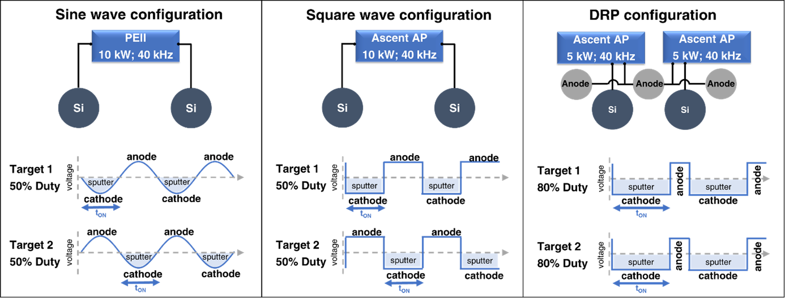
Figure 1. Details on the three bipolar pulsing configurations and the respective power supply units used in this work: sine wave (PEII power supply), square wave (Ascent APâ DMS power supply) and dynamic reverse pulsing (Ascent AP DMS power supply).
Experimental Setup
We performed studies in an industrial drum coater with 600 mm long silicon rotary targets, as shown in Figure 2. All three modes could be tested in this system, so a reliable comparison between the different modes is possible.
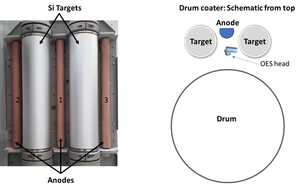
Figure 2: (Left) Process door on the drum coater showing two 600 mm Si targets and the anodes. (Right) Top view of the chamber showing the position of the optical emission spectroscopy (OES) head looking into the plasma in between the two targets from top down.
The targets were sputtered at a total power of 10 kW and pulsing frequency of 40 kHz with Ar gas flow of 100 sccm. For the three modes, nitrogen gas was introduced in the chamber followed by the discharge voltage behavior as shown in Figure 3. Optimization tests showed that, for each mode, 120 sccm of N2 gas flow was required to deposit stoichiometric and transparent silicon nitride films with a refractive index of 2.05 at 550 nm (n and k measured with ellipsometer).
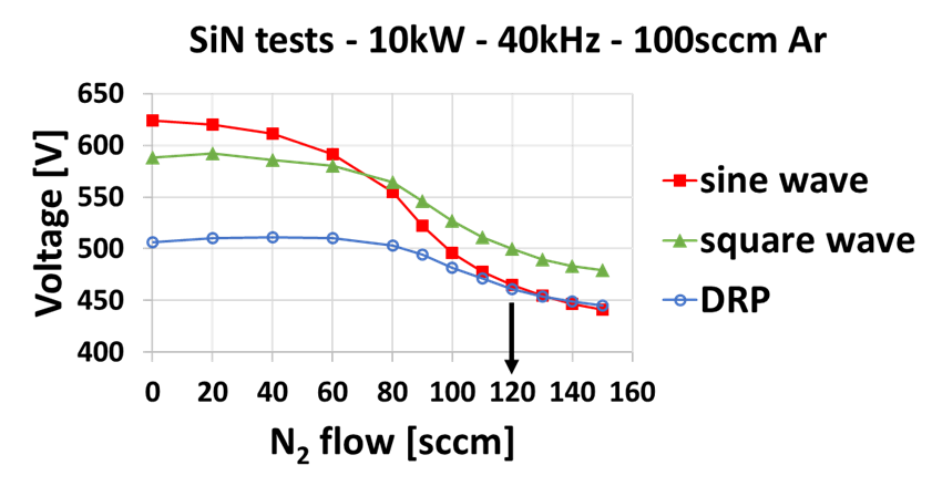
Figure 3. Discharge voltage behavior as a function of N2 flow for the three modes: sine wave, square wave and DRP.
Thus, under the above conditions with 120 sccm of N2 flow, silicon nitride films with 500 nm thickness were deposited on glass substrates at a pressure of 2.8 Bar. The depositions were in dynamic mode at a carrier speed of 1 rpm. Figure 4 shows the results for the power-normalized deposition rate, heat load at the substrate, and the residual stress in the films.

Figure 4: Comparison of the results for silicon nitride deposition (at 10 kW, 40 kHz) showing power normalized dynamic deposition rate (ellipsometer measurement of film thickness), thermal load at the substrate (thermocouples attached to glass substrate on the carrier) and residual stress in the films (substrate curvature method).
Observations
We observed the following:
The deposition rate with the sine wave mode is appreciably lower than the others. In pulsed sputtering, the shapes of the current/voltage waveforms (Figure 5) are determined by plasma decay and re-establishment during each half cycle [1]. Temporal studies have indicated that in square wave mode, fast polarity switching with sharp dU/dt ascertains substantial plasma density at the end of the “off-time” [2, 3], which is then responsible for fast plasma re-establishment upon polarity change to “on-time”. In contrast, in sine wave pulsing with slower polarity switching, the plasma extinguishes and is re-established relatively slower, which may thereby negatively affect the sputter yield at initial low voltages in the pulse. Future studies will delve into this topic further.
.png)
Figure 5. Voltage and current waveforms for sine wave, square wave and DRP modes from this study (10 kW, 40 kHz, Si targets).
DRP mode provided benefits also in terms of heat load and stress, which were considerably lower than those for sine wave and square wave depositions. The latter films (sine and square wave) also exhibit slight delamination, which may be attributed to the high residual stress, while the DRP films adhered well.
Figure 6 shows surface roughness measurements using AFM. It shows a slightly rougher film surface and a different surface structure for the sine wave mode, as compared to square wave and DRP modes.

Figure 6. Atomic force microscopy (AFM) images showing surface features and roughness values for the 500 nm silicon nitride films.
Finally, optical emission spectroscopy (OES) measurements show interesting differences in the plasma behavior. Figure 2 (right) shows the placement of the OES head in the chamber, in between the two targets, to view the plasma from the top. The signal for the N (337 nm) and Ar (825 nm) lines are shown in Figure 7.

Figure 7. OES measurement between the two targets (as shown in Figure 1, right) showing part of the signal specifically for N and Ar lines for the three modes. Note that the scales are similar.
The measurements show two distinct differences:
- The intensities of the N and the Ar lines are slightly higher for the sine wave mode as compared to the square wave mode and both these lines are appreciably lower for the DRP mode.
- Fluctuations in the intensities of the N and Ar lines are seen for both, the sine wave and square wave modes, but not for the DRP mode. These fluctuations correspond to the drum rotation speed of 1 rpm and are thus attributed to plasma interference by the drum.
The similarity between the intensity of the lines and fluctuation behavior for the sine wave and square wave modes indicate that the plasma spreads stronger towards the substrate carrier with both these modes as compared to the DRP mode.
Conclusion
These studies show a firsthand comparison of the influence of different pulse shapes on film properties and showcase inherent differences in plasma behavior during reactive sputter deposition of silicon nitride. Based on deposition rate, substrate heat load, film residual stress and roughness results, DRP mode performs best overall. While sine wave and square wave perform quite similarly, square wave outperforms in terms of deposition rate and surface quality.
Contact us to learn more about the scope of different power configurations and their benefits, or to test them with us at Advanced Energy’s Customer Solutions Lab.
References:
1) J. Bradley and T. Welzel. Physics and phenomena in pulsed magnetrons: an overview. Journal of Physics D: Applied Physics, 42, 2009, 093001.
2) M. List, U. Krause, & T. Wünsche. Dynamic behaviour of unipolar and bipolar pulsed magnetron sputtering. Proceedings of the 44th annual technical conference - society of vacuum coaters, 2001.
3) A. Belkind, Z. Zhao, D. Carter et. al. Pulsed-DC reactive sputtering of dielectrics: pulsing parameter effects. Proceedings of the 43rd annual technical conference - society of vacuum coaters, 2000.
Comparing Three Bipolar Pulsed Power Modes
We compared three different types of bipolar pulsed power modes (Figure 1) for sputter deposition of silicon nitride:
- Sine wave: two targets pulsed against each other, symmetric sinusoidal pulse shape with 50% duty cycle
- Square wave: two targets pulsed against each other, symmetric square pulse shape with 50% duty cycle
- DRP: two targets pulsed in sync against explicit anode, square pulse shape but variable duty cycle (80% used in this study)

Figure 1. Details on the three bipolar pulsing configurations and the respective power supply units used in this work: sine wave (PEII power supply), square wave (Ascent APâ DMS power supply) and dynamic reverse pulsing (Ascent AP DMS power supply).
Experimental Setup
We performed studies in an industrial drum coater with 600 mm long silicon rotary targets, as shown in Figure 2. All three modes could be tested in this system, so a reliable comparison between the different modes is possible.

Figure 2: (Left) Process door on the drum coater showing two 600 mm Si targets and the anodes. (Right) Top view of the chamber showing the position of the optical emission spectroscopy (OES) head looking into the plasma in between the two targets from top down.
The targets were sputtered at a total power of 10 kW and pulsing frequency of 40 kHz with Ar gas flow of 100 sccm. For the three modes, nitrogen gas was introduced in the chamber followed by the discharge voltage behavior as shown in Figure 3. Optimization tests showed that, for each mode, 120 sccm of N2 gas flow was required to deposit stoichiometric and transparent silicon nitride films with a refractive index of 2.05 at 550 nm (n and k measured with ellipsometer).

Figure 3. Discharge voltage behavior as a function of N2 flow for the three modes: sine wave, square wave and DRP.
Thus, under the above conditions with 120 sccm of N2 flow, silicon nitride films with 500 nm thickness were deposited on glass substrates at a pressure of 2.8 Bar. The depositions were in dynamic mode at a carrier speed of 1 rpm. Figure 4 shows the results for the power-normalized deposition rate, heat load at the substrate, and the residual stress in the films.
Figure 4: Comparison of the results for silicon nitride deposition (at 10 kW, 40 kHz) showing power normalized dynamic deposition rate (ellipsometer measurement of film thickness), thermal load at the substrate (thermocouples attached to glass substrate on the carrier) and residual stress in the films (substrate curvature method).
Observations
We observed the following:
| Deposition rate | DRP > square wave >> sine wave |
| Heat load at substrate | sine wave @ square wave >> DRP |
| Residual stress | sine wave @ square wave >> DRP |
The deposition rate with the sine wave mode is appreciably lower than the others. In pulsed sputtering, the shapes of the current/voltage waveforms (Figure 5) are determined by plasma decay and re-establishment during each half cycle [1]. Temporal studies have indicated that in square wave mode, fast polarity switching with sharp dU/dt ascertains substantial plasma density at the end of the “off-time” [2, 3], which is then responsible for fast plasma re-establishment upon polarity change to “on-time”. In contrast, in sine wave pulsing with slower polarity switching, the plasma extinguishes and is re-established relatively slower, which may thereby negatively affect the sputter yield at initial low voltages in the pulse. Future studies will delve into this topic further.
.png)
Figure 5. Voltage and current waveforms for sine wave, square wave and DRP modes from this study (10 kW, 40 kHz, Si targets).
DRP mode provided benefits also in terms of heat load and stress, which were considerably lower than those for sine wave and square wave depositions. The latter films (sine and square wave) also exhibit slight delamination, which may be attributed to the high residual stress, while the DRP films adhered well.
Figure 6 shows surface roughness measurements using AFM. It shows a slightly rougher film surface and a different surface structure for the sine wave mode, as compared to square wave and DRP modes.

Figure 6. Atomic force microscopy (AFM) images showing surface features and roughness values for the 500 nm silicon nitride films.
Finally, optical emission spectroscopy (OES) measurements show interesting differences in the plasma behavior. Figure 2 (right) shows the placement of the OES head in the chamber, in between the two targets, to view the plasma from the top. The signal for the N (337 nm) and Ar (825 nm) lines are shown in Figure 7.

Figure 7. OES measurement between the two targets (as shown in Figure 1, right) showing part of the signal specifically for N and Ar lines for the three modes. Note that the scales are similar.
The measurements show two distinct differences:
- The intensities of the N and the Ar lines are slightly higher for the sine wave mode as compared to the square wave mode and both these lines are appreciably lower for the DRP mode.
- Fluctuations in the intensities of the N and Ar lines are seen for both, the sine wave and square wave modes, but not for the DRP mode. These fluctuations correspond to the drum rotation speed of 1 rpm and are thus attributed to plasma interference by the drum.
The similarity between the intensity of the lines and fluctuation behavior for the sine wave and square wave modes indicate that the plasma spreads stronger towards the substrate carrier with both these modes as compared to the DRP mode.
Conclusion
These studies show a firsthand comparison of the influence of different pulse shapes on film properties and showcase inherent differences in plasma behavior during reactive sputter deposition of silicon nitride. Based on deposition rate, substrate heat load, film residual stress and roughness results, DRP mode performs best overall. While sine wave and square wave perform quite similarly, square wave outperforms in terms of deposition rate and surface quality.
Contact us to learn more about the scope of different power configurations and their benefits, or to test them with us at Advanced Energy’s Customer Solutions Lab.
References:
1) J. Bradley and T. Welzel. Physics and phenomena in pulsed magnetrons: an overview. Journal of Physics D: Applied Physics, 42, 2009, 093001.
2) M. List, U. Krause, & T. Wünsche. Dynamic behaviour of unipolar and bipolar pulsed magnetron sputtering. Proceedings of the 44th annual technical conference - society of vacuum coaters, 2001.
3) A. Belkind, Z. Zhao, D. Carter et. al. Pulsed-DC reactive sputtering of dielectrics: pulsing parameter effects. Proceedings of the 43rd annual technical conference - society of vacuum coaters, 2000.
Gayatri Rane
Advanced Energy
As an R&D scientist at AE, with past experience in sputtering and thin film analysis, I am involved with the research activities of the Customer Solutions Lab in Karlstein am Main, Germany.
More posts by Gayatri Rane
